Hello,

Per "Table 6.2: Recommended Power Operating Range" in BL702 Datasheet (6.2.1 Power characteristics) VDDIO_2 could be from 1.8V to 3.63V with typical value 3.3V. But in all other places of datasheet VDDIO_2 specified to be supplied with exactly 3.3V and no other values are supposed to be allowed:

I want to use GPIO9 pin as ADC input. Could I supply VDDIO_2 with 2.5V in this case?

Could VDDIO_2 be supplied with full range of supply voltages (1.8V to 3.3V) and there is an error in datasheet figures or 3.3V requirements are caused by hardware restrictions?

    Power characteristics from datasheet:

      I've saw this table, but did you try BL702 with lower VDDIO2 voltages? Especially I'm interested in proper internal DC/DC functioning, cause chinese hardware design guide tells us:

      Pin14(VDDIO2): digital part and DCDC module power supply, the typical input voltage is 3.3V.

      So I have some doubts about how internal DC-DC will perform with VDDIO2 lower than 3.3V and especially with 1.8V. Could you clear this up?

        "the typical input voltage is 3.3V" means from 1.8V to 3.63V.

        I think only AVDD33_RF with AVDD33_PA need 3.3V to achive maximum +14dBa transmit power. Normally they get 1.5V from DC-DC converter.

        And don't forget, internal flash operating voltage can be 2.3V and above. Surprise!
        That's why reset circuit installed in XT-ZB1 module.

        The results of the measurements will be clear after appropriate experiments.

        • makc replied to this.

          Suprise, there is no AVDD33_RF in pinout, it presents only in "Table 4.2: Recommended Power Operating Range".

          Delicates And don't forget, internal flash operating voltage can be 2.3V and above. Surprise!

          Yes, I've read this note. But as I can understand, this restriction is applied only to the VDDIO_1.

            AVDD_RF = AVDD33_RF. Documentation is very poor and full of mistakes.
            AVDD33_PA - RF Power Amplifier power supply pin.

              makc I think that simple RC-circuit is enough for proper reset.

              You can try it anyway. It is unlikely that something can be damaged. But stable work of this device is not guaranteed below operating voltage of internal flash. The CPU may start before the flash memory.

                "The reset of BL70X can use the PU_CHIP pin. When the PU_CHIP is low (less than 0.8V), the chip resets. When the PU_CHIP is high (above 2.0V), the chip is in working state."

                Chip starts at 2.0V, but internal flash can start from 2.3V or above!

                • makc replied to this.

                  Delicates
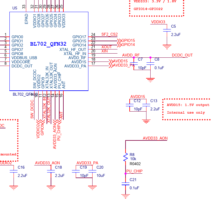
                  The question is VDD ramp time and RC-net time constant, given values from above example (C=0.1u, R=10k), 1.6 ms soft-start time from main DC/DC VDD power supply it will take about more than 1 ms to get PU_CHIP voltage above 2.0V:

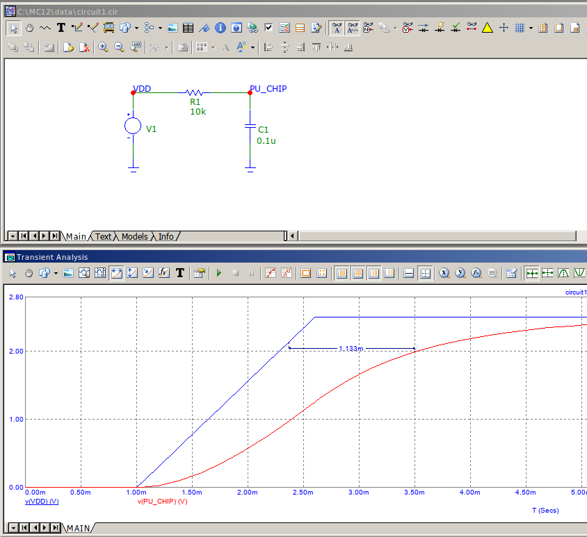
                  Do you suppose, that something could go wrong in this case? I doubt it.

                  Reset supervisor in mentioned Bluetooth module is quite good decision, but in my case there is no space on board for it and I have no wish to pay for it. ;-)

                  makc You understand what to do and can read the instructions, but many people do not and make a lot of mistakes. For example, they try to start their BL70X device at an operating voltages of 1.8 - 2.3 volts.

                    AVDD33_AON - Always ON power supply. And VDDIO_2 connected to it because interrupt from GPOP9-12 can wake up CPU from Sleep mode (HBN).

                      Write a Reply...
                      @ 2025 Bouffalo Lab (Nanjing) Co., Ltd. All rights reserved.